Printed Circuit Boards
All my electrical and computer engineering related projects thus far have been built on breadboards. This is a great way to explore and debug a circuit or system one is working on. Once the prototype is finished, it can be transferred onto a printed circuit board (PCB). PCBs are layers of conductive and insulated materials that connect each circuit component in a controlled and permanent manner. The production of PCBs is an intricate and involved process, but it all starts with the design of the circuit that is to be implemented.
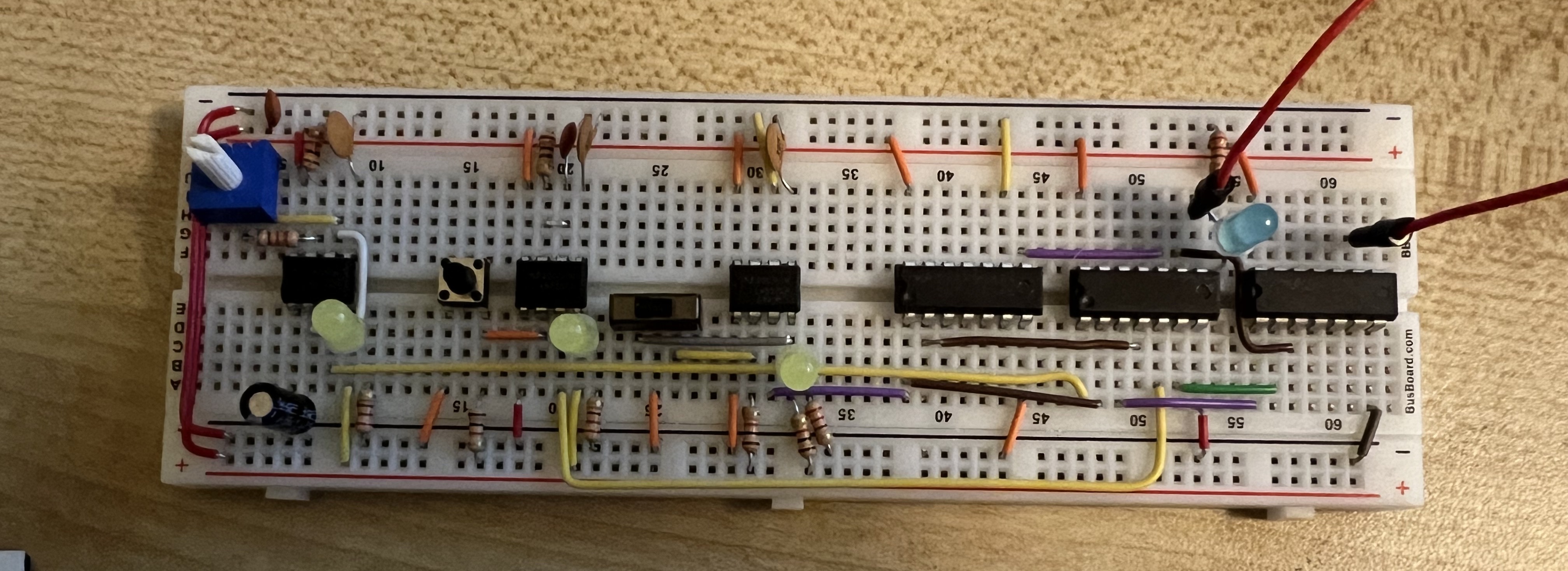
Up to this point, I have had no formal class on PCBs but wanted to learn more about them. I decided to hit the ground running and design my own PCB and have it fabricated. An easy enough start was to take a clock module and move it to a PCB. The clock module creates a clock pulse for prototyping computer systems, mainly used on the 6502 Computer and the Breadboard Video Card. It allows two different output types: steady pulse where the frequency is controlled by the potentiometer and a single step pulse which is controlled by the push button. This clock module uses the IC555 and the breadboard implementation is seen in the image below.
Design
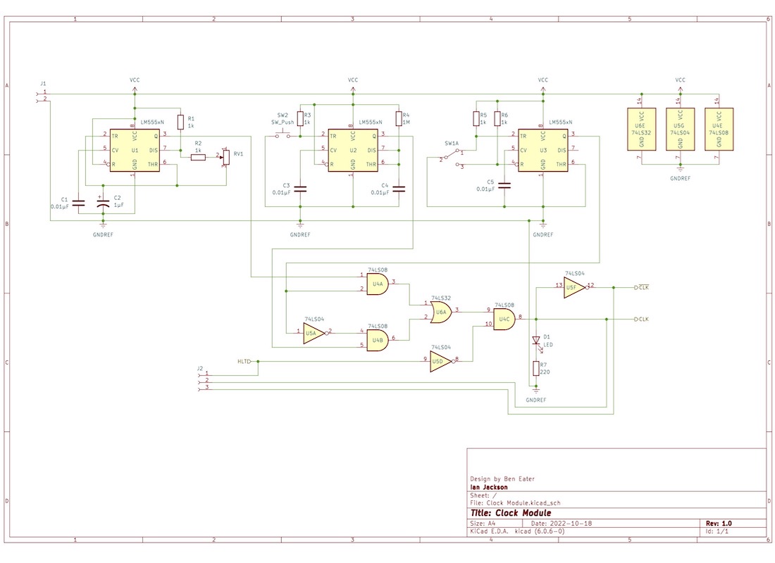
The first step is to draw up the schematic in KiCAD. This schematic can be seen in the image slides below. Once the schematic was finished, it was time to get into the PCB work. Each component in the schematic needed a footprint. A footprint is how the software determines the sizing and placement of the through holes for the component. Since I have all of the components, I chose to use through hole technology (THT) footprints, meaning the element's legs are stuck though the holes and soldered in place. The other option is surface mounted devices (SMDs). This is how you see most circuit components mounted in professional work. I do not have the SMD package of the components for this project, nor the equipment to place them on the board. Maybe next time.
Place and Route
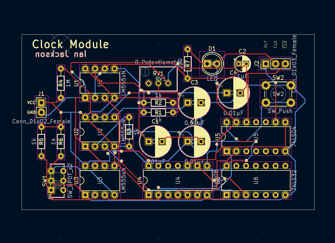
After selecting a footprint for each component, it is time to move into the PCB editor in KiCAD. Here is where these 2D footprints are placed on a sheet and free to move around. Each component is arranged into a desired location. Once the footprints are placed, it is time to route. Routing is the process in which the physical connections between the elements are laid out. The whole process of placing footprints and routing connections is given the name "place and route."
There are a lot of things to take into consideration when it comes to place and route. The ideal PCB will have circuit element placement that reduces the wire distance which in turn reduces power consumption and doesn't violate timing constraints. There are professional softwares out there that do this work automatically. As a college student who wants to learn about PCBs on their own with a simple circuit, these considerations are not as much of a worry.
Putting it Together
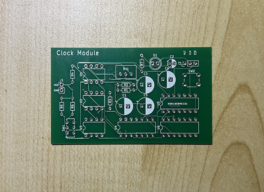
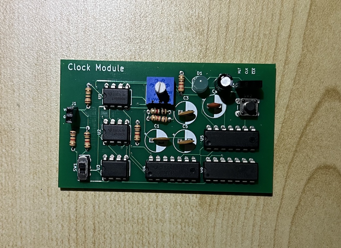
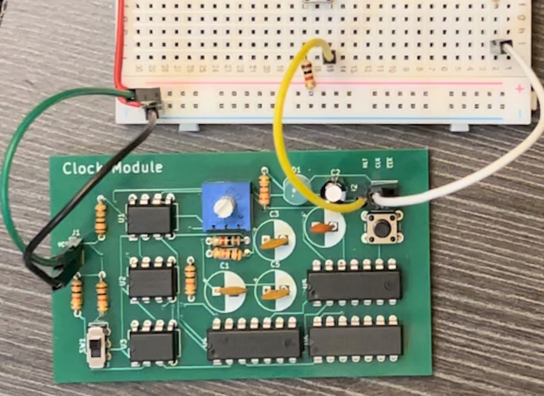
Design is done, place and route is done, and KiCAD ran checks to ensure all connections are made. Now it is time to fabricate the PCB. I had PCBWay fabricate and ship my design. After a couple of weeks, I received blank PCB boards of my design! The blank board is seen in the third image below. After soldering 110 connections, the PCB is finished and is seen in the fourth slide.
The last slide below shows a demonstration of the PCB in work. It shows the clock creating a constant pulse changing with the potentiometer. It then switches to the single step mode. The output of the clock is connected to an external LED to show the output ports. The external button on the breadboard is the hault input. When this is high, the clock pulse is haulted.
